
The new chip incorporates a dual-core architecture with RISC-V vector acceleration and reaches 1.5 GHz using Intel 18A technology, reinforcing the roadmap toward high-performance processors
BZL has reached a new milestone in the development of the Cinco Ranch processor family with the submission of Test Chip 2 (TC2) for manufacturing. This advance represents a key step in the Cinco Ranch roadmap, a family of processors based on the open RISC-V architecture designed to drive new generations of high-performance computing. Building on the experience gained with the first Test Chip (TC1), the team of chip design experts involved in BZL continues to move forward toward more complex designs.
The architecture of the chip family known as Cinco Ranch encompasses two generations of test chips: TC1 and TC2, each aimed at validating different levels of integration and computational capacity. While TC1 was designed as a single-core processor, TC2 introduces a dual-core architecture with greater processing capabilities.
Cinco Ranch TC2: a leap toward a more advanced architecture
The Cinco Ranch TC2 represents a significant evolution from the first test chip. Its architecture includes:
- Two processing cores, each composed of the Lagarto Ox out-of-order scalar processor and the Valyria vector accelerator.
- Three levels of cache memory on-chip to improve system performance and efficiency.
- The vector processing unit (VPU) in each core features eight lanes, each equipped with four floating-point units (FPUs). It supports the RISC-V Vector 1.0 (RVV 1.0) extension.
In addition to the CPU subsystem described above, the chip includes a series of auxiliary blocks essential for its operation, notably:
- Two PCIe links: each link has a PCIe Gen4 digital controller and a physical interface with two lanes each.
- LPDDR5 (DDR) interface: digital controller and physical interface for external LPDDR5-6400 memory with 4 channels of 16 bits each.
- Peripherals for external components: SD card, UART, non-volatile memory (eFuse), SPI, I2C, GPIO.
- Several PLL blocks for generating the high-speed clocks needed by other subsystems.
- Network on Chip (NoC): interconnection logic between the different subsystems and the CPUs.
The CPU improvements represent progress toward a processor capable of handling more intensive workloads, bringing the architecture developed by BZL closer to the requirements of future scientific computing and artificial intelligence systems.
Validated design ready for advanced manufacturing
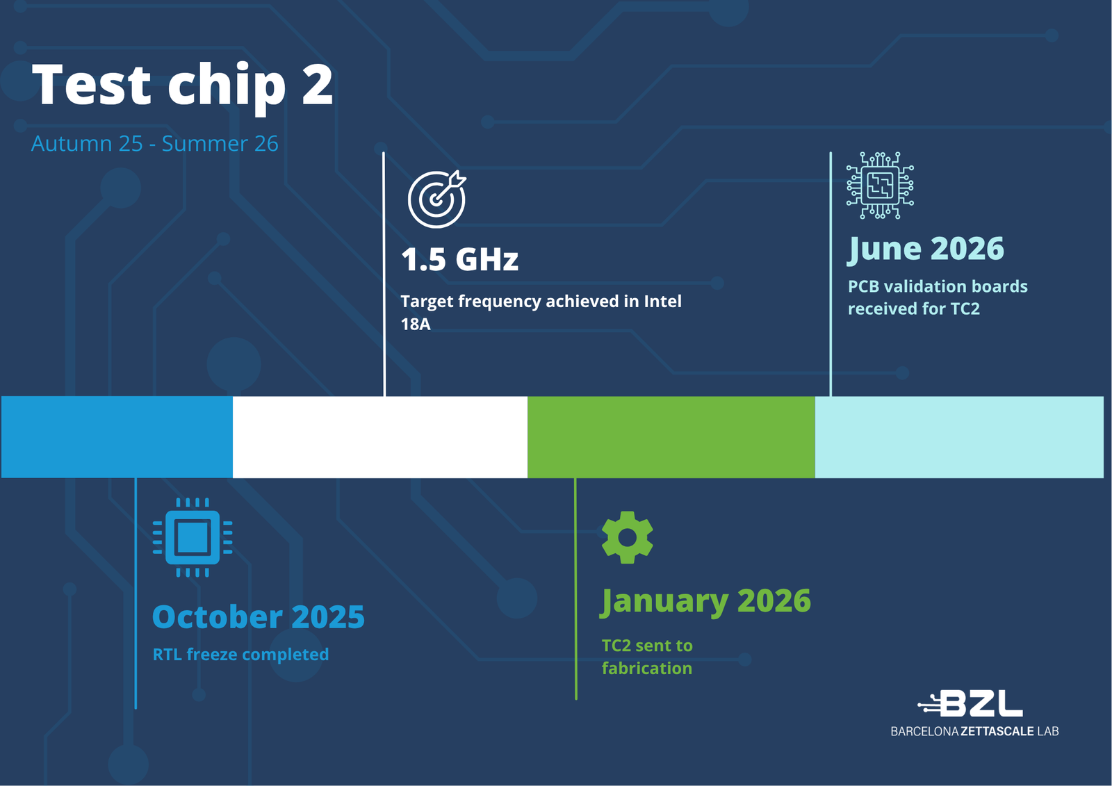
The BZL team completed the TC2 RTL in October 2025, closing out the chip design definition before it was sent to manufacturing in January 2026. During this phase, a detailed analysis of the design’s critical paths was carried out to optimize performance on Intel 18A technology, enabling the TC2 to reach a target frequency of 1.5 GHz. The development also incorporated advanced tools for inserting Design for Test (DFT) and Memory Built-In Self-Test (MBIST) capabilities, key elements for facilitating the chip’s validation and diagnosis during later testing phases.
Following submission to manufacturing, the BZL team continues working on software development and preparing the bring-up of the Cinco Ranch TC2 — the phase in which the fabricated chip will be powered up for the first time and its physical operation validated. As part of this preparation, the validation PCB boards are expected to arrive at the end of April, a necessary step to begin experimental testing of the new processor.
The development of the Cinco Ranch TC2 reinforces BZL’s strategy of moving toward open, scalable processors designed for the future needs of supercomputing and AI. The evolution from TC1 to TC2 and future designs reflects a progressive roadmap toward increasingly complex architectures, from multi-core solutions to multi-core systems with advanced vector acceleration. With this new milestone, BZL continues to contribute to the development of proprietary semiconductor technologies and to strengthening the RISC-V-based processor ecosystem.